InP
Substrates
Manufacturers
Epitaxial Wafers
Selective Area Growth (SAG) butt joint growth : a PhD thesis 2019 TU Eindhoven Univ. Tech.
Manufacturers
Device Design & Fabrication
- Semiconductor lasers and fiber optics
- DFB Laser (Wikipedia)
- DFB laser structure
- Major fabrication processes for InP lasers (by DeepSeek)
- No- regrowth EML : Selective Area Growth or Quantum Well Intermixing, identical activity EML Korea 2024
- New laser lays groundwork for next generation ethernet technology (EML 200 Gbps, Lumentum Japan 2023)
- 200 Gb/s Uncooled EML with Single MQW Layer Stack Design (Fraunhofer HHI 2022)
- 50 GB EML (with some fabrication process details, Institute of Semiconductors, China, 2022)
- InP-Components for 100 GBaud Optical Data Center Communication (2021, Fraunhofer Heinrich Hertz Institute )
- Integrated transmitter devices on InP exploiting electro-absorption modulation (2020)
- 100GBaud+ Silicon Photonics Solutions Drive Optical Network Evolution (2020)
- Wide-temperature-range 100-Gbaud Operation of a Lumped- electrode-type EA-DFB for an 800-Gb/s (Lumentum Japan, 2020)
- EML design and improvements from Mitsubishi 2022
- DFB laser fabrication (NTT 2010)
- How to Create a Laser Model for a Photonic Process Design Kit (PDK, Ansys)
III-V on silicon electroabsorption modulators (Ghent Univ.) |
Manufacturers
- Coherent (US)
- Lumentum (US)
- Broadcom
- MACOM (making InP laser in 4-inch GaAs line)
- Fraunhofer HHI Berlin InP foundry (Germany)
- Sivers (Foundry, Sweden, Sivers Photonics : Glasgow UK)
- GCS : GaAs & InP foundry (Taiwan)
- InPho (Canada)
- Albis (InGaAs/InP and GaAs photodiodes , Switzerland)
- Thorlabs (US)
- Almae (France)
- Chilas BV Hybrid-integration external cavity laser (ECL, The Netherland)
- LioniX International (The Netherlands) offers ultra-low loss Photonic integrated circuits (PICs) and custom-made modules based on silicon nitride.
Equipment
InP wafer scriber
Packaging
- Chilas B.V.
- EU TwiLight Project
- InP & Silicon Photonics : heterogeneous integration or hybrid integration ? (2018)
Manufacturers
Testing
- Quantifi Photonics (Formerly known as Coherent Solutions, HQs New Zealand; N. America, Thailand )
- InP HBT for testing equipment
Modules and Applications
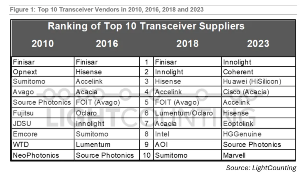
- Major Optical transceiver produces :

InP info post
- InP AND III-V COMPOUNDS (Roadmap 2020, good description for equipment and processes ). Article in pdf
- Photonic integrated circuit (wikipedia)
- Electro-absorption modulator (Wikipedia)
- 1.3-µm identical active electro-absorption modulated laser with quantum well intermixed passive waveguide (2024)
- Coherent Achieves World’s First 6-inch InP Wafer (2024)
- Coherent expands capacity in US and Europe (2024)
- Indium phosphide industry moving into consumer applications (Yole 2022)
- Design of a 200Gbps externally modulated laser for opto-electronic integration (simulation, Master Thesis, Sweden, 2022)
- AlGaInAs/InP EML with Sidewall Grating Distributed Feedback Laser and Quantum Well Intermixing Technology (2022)
- 1.3 µm InGaAlAs/InP laser integrated with laterally tapered SSC in a reverse mesa shape (2021)
- Optimal Design of High-Speed Electro-Absorption Modulated Laser Based on Double Stack Active Layer Structure (2021)
- Integrated transmitter devices on InP exploiting electro-absorption modulation (2020)
- High Power and High Efficiency Operation of Semiconductor Optical Amplifier Assisted Extended Reach Electroabsorption Modulated DFB Laser (AXEL) for Extension of Transmission Distance (NTT, 2019)
- Fraunhofer Berlin InP foundry talk video (2018)
- Integration of Photonics and Electronics at Eidenhoven Univ. (video 2018)
- Manufacturing InP lasers and GaAs devices in the same 4-inch production line (Macom 2018) Article in pdf
- Fabrication of InP-based monolithically integrated laser transmitters (2018)
- Fabrication of InP-based monolithically integrated laser transmitters (A review article, 2018)
- EML Array fabricated by SAG technique monolithically integrated with a buried ridge AWG multiplexer (2017)
- Reflecting on PIC manufacturing solutions (2017)
- Method for fabricating an elctro-absorption modulated laser and electro-absorption modulated laser (2017)
- EMCORE Expanding Production of Breakthrough Linear Externally Modulated Laser (L-EML™)-Based Transmitters (2016)
- Fabrication of an electro-absorption modulated distributed feedback laser by quantum well intermixing with etching ion-implantation buffer layer (2015)
- Ten-channel InP-based large-scale photonic integrated transmitter fabricated by SAG technology (2015)
- 1.55 µm high speed low chirp electroabsorption modulated laser arrays based on SAG scheme (2014)
- Manufacturing Progress for InP-based 500 Gb/s Photonic Integrated Circuits (2013)
- Wide Temperature Operation of 40 Gbps 1550 nm Electroabsorption Modulated Lasers (2005)
- InP laser diode device production: DFB Grating Etch for maximum performance (Oxford White Paper)
Leave a Reply
You must be logged in to post a comment.